2018年9月5日水曜日

si5351a VXO

VXOとVFOとの切り分けが難しいが、VXOはアナログ信号を利用したもので、表示器なしと勝手に定義。コントロールにはPIC112F1840を使い、si5351aの発振周波数にADCにボリュームを繋ぎ、加減算する事で周波数調整を行うVXOとした。アナログ入力を使用した時、 目標周波数=発振周波数+ADC値 で簡単に計算する事ができる。PIC12F1840のADCは10Bitの為、0から1023の変化量が得られる。従って、分解能1Hzとした場合、発振周波数+1023(Hz)の変化になる。

回路図

si5351a Xtal代替発振器の回路図通り。

ボリューム変化量

10BitのADCの為、0-1023の値を持つ。この為、発振周波数+1023 が目標周波数でであれば簡単だが、VXOとして使える範囲が限定される。そこで、水晶発振子を使ったVXOと同等な性能を目指す事にした。目標可変範囲を±30kHzとした。これをADC分解能で現すと±30倍スケーリングしなければならない。1Bitの変化が30Hzとして計算されるので、ADCによる変換誤差、外来ノイズなど顕著に周波数に反映された結果、周波数が揺らぐ。この揺らぎは、5倍のスケーリングした時でも受信機にトーン変化として感じられた。使い勝手と揺らぎ有無判断から、ADC値2倍のスケーリング(分解能 2Hz)を行うことにした。従って、ADC*2(0-2046)がボリューム変化量となる。

周波数中心値

ADC値を2倍した値をボリュームの最小位置から最大位置として使うので、ボリューム中心値を発振周波数(初期値)と操作性が良い。そこでオフセット 発振周波数ー1023 にした。

可変範囲拡張方法

今迄の説明で、発振周波数±1023 即ち、発振周波数±1kHz変化する事が想像出来た思うが、30kHz程安定して可変させるには工夫がいる。SSB運用形態を観ていると、1kHzステップ刻みが多い。そこで1kHzスキップさせる為、SKIP SWを付けた。SKIPを押すと、+1kHzまたは-1kHzスキップさせる事にした。+またはー判断は、ボリュームの中心値を基準に大小判断にした。SKIPを押す度にEEPROMに周波数を保存して可変範囲を拡張した。このVXOを仮称「GQP VXO」と呼ぶ。

EEPROM初期化の方法

表示器を持たないシステムの場合、初期化は重要である。SKIP SWを押しながら電源スイッチを投入すると、EEPROMが初期化される方式にした。(初めて使う時は、初期化が必要)

スケッチ

Mplab X X8Cを使って開発を行った。スケッチはJA2GQP's Download siteのPICフォルダからダウンロード可能。

////////////////////////////////////////////////////////////
//    si5351a PLL control(PIC12F1840)
//
//                                    2018/09/03
//                                    JA2GQP   
////////////////////////////////////////////////////////////


//---------- Header file include -------------------------//

#include <xc.h>

//----------Configuration setting ------------------------//

////////////////////////////
// config1
////////////////////////////
#pragma config FOSC     = INTOSC            // Internal clock
#pragma config WDTE     = OFF               // Watchdog timer off
#pragma config PWRTE    = ON                // Power on start
#pragma config MCLRE    = OFF               // External reset not used
#pragma config CP       = OFF               // Program memory not protected
#pragma config CPD      = OFF               // Data memory not protected
#pragma config BOREN    = ON                // Power drop monitoring
#pragma config CLKOUTEN = OFF               // Clock out pin is RA4
#pragma config IESO     = OFF               // No activation with clock switching
#pragma config FCMEN    = OFF               // Do not monitor external clock

////////////////////////////
// config2
////////////////////////////
#pragma config WRT      = OFF               // Flash memory not protected
#pragma config PLLEN    = OFF               // It does not work at 32 MHz
#pragma config STVREN   = ON                // Reset with stack overflow(underflow)
#pragma config BORV     = HI                // Voltage drop monitoring
#pragma config LVP      = OFF               // Low voltage programming not used

//---------- Define value setting ------------------------//

#define DEF_FREQ        14000000-AD_OFFSET  // Default frequency
#define EEP_ADR         0x00                // EEPROM address
#define SCL   RA1                           // I2C Clock
#define SDA   RA2                           // I2C Data
#define AD_OFFSET       1023                // Frequency offset
#define _XTAL_FREQ      16000000            // clock 16MHz(Use with delay)

////////////////////////////
// si5351a parameter
////////////////////////////
#define CLK0_CTRL     16                    // Register definitions
#define CLK1_CTRL     17
#define MSNA_ADDR     26
#define MS0_ADDR      42
#define PLL_RESET    177
#define XTAL_LOAD_C  183
#define R_DIV_1      0b00000000             // R-division ratio definitions

#define Si5351A_ADDR  0xC0                  // address(cip address<<1)
#define XTAL_FREQ     25000000              // Crystal frequency for Hans' board

#define _6pF          0b01010010            // 6pF
#define _8pF          0b10010010            // 8pF
#define _10pF         0b11010010            // 10pF
#define XTAL_CL       _8pF                 // XTAL_CL 8pF set

#define _2mA           0x4C                 // 2mA(1dBm))
#define _4mA           0x4D                 // 4mA(5dBm))
#define _6mA           0x4E                 // 6mA(10dBm))
#define _8mA           0x4F                 // 8mA(12dBm)
#define mA            _6mA                  // output lebel 10dBm set

//---------- Memory define -------------------------------//

static unsigned long  frequency=DEF_FREQ;   // Frequency data

//------------- Initial proc. ----------------------------//

void PIC12F1840_set(){
    OSCCON     = 0b01111000 ;               // clock set(16MHz=0x78,8MHz=0x70,4MHz=0x68)
    ANSELA     = 0b00010000 ;               // Anarog = AN3,Othe digital
    TRISA      = 0b00011000;                // I/O set(0=output,1=input)
    PORTA      = 0b00000000 ;               // Output pin initial value

    EECON1bits.CFGS =0;                     // EEPROM
    EECON1bits.EEPGD = 0;

    ADCON1     = 0b11010000 ;               // FOSC/16,VDD=Ref
    ADCON0     = 0b00001101 ;
    __delay_us(5) ;                         // 5us(at clock 16MHz))
}

//------------- wait proc. -------------------------------//

void await(unsigned long ct){
  while(ct>0) ct--;
}

//------------- I2C start proc. --------------------------//

void I2C_start(){
    SCL = 1;                                // start condition
    await(3);
    SDA = 1;
    await(3);
    SDA = 0;
    await(3);
    SCL = 0;
    await(3);
 }

//------------- I2C stop proc. ---------------------------//

void I2C_stop(){
    await(3);
    SCL = 1;                                // stop condition
    await(3);
    SDA = 0;
    await(3);
    SDA = 1;
    await(3);
    SCL = 0;
    await(3);
 }

//------------- I2C write byte proc. ---------------------//

void wr_Byte(unsigned char x){
    unsigned int k;
    for(k=0;k<8;k++){
        if(x & 0x80) SDA = 1; else SDA = 0;
        await(3);
        SCL = 1;
        await(3);
        SCL = 0;
        await(3);
        SDA = 0;
        x <<= 1;
    }
    SCL = 1;
    await(3);
    SCL = 0;
}

//------------- si5351 command processing ----------------//

void Si5351_write(unsigned char reg_No, unsigned char x){
    I2C_start();

    wr_Byte(Si5351A_ADDR);                  // address set
    wr_Byte(reg_No);
    wr_Byte(x);

    I2C_stop();
}

//------------- si5351 Initialization --------------------//

void Si5351_init(void){
    SDA=1;
    SCL=1;

    await(200);
    Si5351_write(XTAL_LOAD_C,XTAL_CL);      // XTAL_CL set
    Si5351_write(CLK0_CTRL,0x80);           // Disable CLK0
    Si5351_write(PLL_RESET,0xA0);           // Reset PLL_A
     
    Si5351_write(CLK0_CTRL,mA);
}

//------------- si5351 PLL data set --------------------------//

void setupPLL(unsigned char pll, unsigned char mult, unsigned long num, unsigned long denom){
  unsigned long P1;                         // PLL config register P1
  unsigned long P2;                         // PLL config register P2
  unsigned long P3;                         // PLL config register P3

  P1 = (unsigned long)(128 * ((float)num / (float)denom));
  P1 = (unsigned long)(128 * (unsigned long)(mult) + P1 - 512);
  P2 = (unsigned long)(128 * ((float)num / (float)denom));
  P2 = (unsigned long)(128 * num - denom * P2);
  P3 = denom;

  Si5351_write(pll + 0, (P3 & 0x0000FF00) >> 8);
  Si5351_write(pll + 1, (P3 & 0x000000FF));
  Si5351_write(pll + 2, (P1 & 0x00030000) >> 16);
  Si5351_write(pll + 3, (P1 & 0x0000FF00) >> 8);
  Si5351_write(pll + 4, (P1 & 0x000000FF));
  Si5351_write(pll + 5, ((P3 & 0x000F0000) >> 12) | ((P2 & 0x000F0000) >> 16));
  Si5351_write(pll + 6, (P2 & 0x0000FF00) >> 8);
  Si5351_write(pll + 7, (P2 & 0x000000FF));
}

//------------- Set up MultiSynth --------------------------//

void setupMultisynth(unsigned char synth, unsigned long divider, unsigned char rDiv){
  unsigned long P1;                         // Synth config register P1
  unsigned long P2;                         // Synth config register P2
  unsigned long P3;                         // Synth config register P3

  P1 = 128 * divider - 512;
  P2 = 0;                                   // P2 = 0, P3 = 1 forces an integer value for the divider
  P3 = 1;

  Si5351_write(synth + 0, (P3 & 0x0000FF00) >> 8);
  Si5351_write(synth + 1, (P3 & 0x000000FF));
  Si5351_write(synth + 2, ((P1 & 0x00030000) >> 16) | rDiv);
  Si5351_write(synth + 3, (P1 & 0x0000FF00) >> 8);
  Si5351_write(synth + 4, (P1 & 0x000000FF));
  Si5351_write(synth + 5, ((P3 & 0x000F0000) >> 12) | ((P2 & 0x000F0000) >> 16));
  Si5351_write(synth + 6, (P2 & 0x0000FF00) >> 8);
  Si5351_write(synth + 7, (P2 & 0x000000FF));
}

//------------- si5351 data set --------------------------//

void si5351aSetFrequency(unsigned long frequency){
  unsigned long pllFreq;
  unsigned long xtalFreq = XTAL_FREQ;
  unsigned long l;
  float f;
  unsigned char mult;
  unsigned long num;
  unsigned long denom;
  unsigned long divider;

  divider = 900000000 / frequency;          // Calculate the division ratio. 900,000,000 is the maximum internal
                                            // PLL frequency: 900MHz
  if (divider % 2) divider--;               // Ensure an even integer
                                            //division ratio

  pllFreq = divider * frequency;            // Calculate the pllFrequency:
                                            //the divider * desired output frequency

  mult = pllFreq / xtalFreq;                // Determine the multiplier to
                                            //get to the required pllFrequency
  l = pllFreq % xtalFreq;                   // It has three parts:
  f = l;                                    // mult is an integer that must be in the range 15..90
  f *= 1048575;                             // num and denom are the fractional parts, the numerator and denominator
  f /= xtalFreq;                            // each is 20 bits (range 0..1048575)
  num = f;                                  // the actual multiplier is mult + num / denom
  denom = 1048575;                          // For simplicity we set the denominator to the maximum 1048575

                                            // Set up PLL A with the calculated  multiplication ratio
  setupPLL(MSNA_ADDR, mult, num, denom);
                                            // Set up MultiSynth divider 0, with the calculated divider.
                                            // The final R division stage can divide by a power of two, from 1..128.
                                            // reprented by constants SI_R_DIV1 to SI_R_DIV128 (see si5351a.h header file)
                                            // If you want to output frequencies below 1MHz, you have to use the
                                            // final R division stage
  setupMultisynth(MS0_ADDR, divider, R_DIV_1);
}

//------------- ADconverter ------------------------------//

unsigned int adconv(){
    unsigned int temp;

    GO_nDONE = 1 ;                          // Anarog read start
    while(GO_nDONE) ;                       // PIC wait
    temp = ADRESH ;                         // Data high set
    temp = ( temp << 8 ) | ADRESL ;         //      low set

    return temp * 2 ;                       // (0-1023) * 2 = 0-2046
}

//------------- EEPROM read ------------------------------//

unsigned long eep_rd(unsigned char address){
    unsigned long temp = 0;

    temp = eeprom_read(address+3);
    temp = temp << 8;
    temp = temp | eeprom_read(address+2);
    temp = temp << 8;
    temp = temp | eeprom_read(address+1);
    temp = temp << 8;
    temp = temp | eeprom_read(address+0);
 
    return temp;
}

//------------- EEPROM write -----------------------------//

void eep_wt(unsigned char address,unsigned long frequency){
    eeprom_write(address+0,(frequency & 0xff));
    eeprom_write(address+1,((frequency >> 8) & 0xff));
    eeprom_write(address+2,((frequency >> 16) & 0xff));
    eeprom_write(address+3,((frequency >> 24) & 0xff));
}

//------------- EEPROM initialize -----------------------------//

void eep_init(){
    if(RA3 == 0){
        while(RA3 == 0)
            ;
        eep_wt(EEP_ADR,frequency);
        eeprom_write(0x0f,0x49);
    }

    if(eeprom_read(0x0f) == 0x49)
        frequency =  eep_rd(EEP_ADR);
}

//------------- main -------------------------------------//

void main(){
    int wk,wk1,i;
    char skip;

    eep_init();
    PIC12F1840_set();                       // Cip Initialization
    Si5351_init();                          // si5351a Initialization

    while(1){
        wk = adconv();

        if(RA3 == 0){
            if(wk < 1024)
                frequency = frequency - 1000;
            else
                frequency = frequency + 1000;

            eep_wt(EEP_ADR,frequency);
            si5351aSetFrequency(frequency + wk);  // Frequency data set
            while(RA3 == 0)
                ;
        }
        else{
            if(wk != wk1){
                si5351aSetFrequency(frequency + wk);  // Frequency data set
                wk1 = wk;
            }
        }

        __delay_ms(30); 
    }
}


2018年8月31日金曜日

si5351a Xtal代替発振器

si5351aをpic12f1840でコントロールしたX'tal代替発振器である。S/W I2Cコントロールを行っており、JE1AHW内田OMの「クリスタルもどきの製作」を参考にさせて頂いた。開発用ボードは、試験が容易な構造にした。si5351aを発振させた場合、PLLである為に周波数の微調整が難しい。今回、周波数のキャリブレーションを容易にする為、ポテンションメータで周波数の微調整(±1kHZ)が出来る様にした。


回路図


電源電圧3.3Vとし、レベルコンバータなしでI/F出来る様にした。試験では、si5351aボードにレベルコンバータ回路が搭載されたボードを使った。出力は、1chのみ。多回転半固定ボリュームを使うと小型化できると思う。
SKIP SWは、今回のスケッチでは使ってない。


スケッチ

目標周波数をボリューム中心値となる様、周波数オフセットを行っている。ADC分解能が10Bitなので、1023*2を周波数データに加えている。従って、発振周波数=目標周波数-オフセット値(1023)+AD値(0-2026)となっている。開発は、Mplab X X8Cを使った。
必要なファイルは、JA2GQP's Download sitePICフォルダからダウンロードできる。

////////////////////////////////////////////////////////////
//    si5351a PLL control(PIC12F1840)
//
//                                    2018/9/3
//                                    JA2GQP     
////////////////////////////////////////////////////////////


//---------- Header file include -------------------------//

#include <xc.h>

//----------Configuration setting ------------------------//

////////////////////////////
// config1
////////////////////////////
#pragma config FOSC     = INTOSC            // Internal clock
#pragma config WDTE     = OFF               // Watchdog timer off
#pragma config PWRTE    = ON                // Power on start
#pragma config MCLRE    = OFF               // External reset not used
#pragma config CP       = OFF               // Program memory not protected
#pragma config CPD      = OFF               // Data memory not protected
#pragma config BOREN    = ON                // Power drop monitoring
#pragma config CLKOUTEN = OFF               // Clock out pin is RA4
#pragma config IESO     = OFF               // No activation with clock switching
#pragma config FCMEN    = OFF               // Do not monitor external clock

////////////////////////////
// config2
////////////////////////////
#pragma config WRT      = OFF               // Flash memory not protected
#pragma config PLLEN    = OFF               // It does not work at 32 MHz
#pragma config STVREN   = ON                // Reset with stack overflow(underflow)
#pragma config BORV     = HI                // Voltage drop monitoring
#pragma config LVP      = OFF               // Low voltage programming not used

//---------- Define value setting ------------------------//

#define DEF_FREQ        14000000-AD_OFFSET  // Default frequency
#define EEP_ADR         0x00                // EEPROM address
#define SCL   RA1                           // I2C Clock
#define SDA   RA2                           // I2C Data
#define AD_OFFSET       1023                // Frequency offset
#define _XTAL_FREQ      16000000            // clock 16MHz(Use with delay)

////////////////////////////
// si5351a parameter
////////////////////////////
#define CLK0_CTRL     16                    // Register definitions
#define CLK1_CTRL     17
#define MSNA_ADDR     26
#define MS0_ADDR      42
#define PLL_RESET    177
#define XTAL_LOAD_C  183
#define R_DIV_1      0b00000000             // R-division ratio definitions

#define Si5351A_ADDR  0xC0
#define XTAL_FREQ     25000000              // Crystal frequency for Hans' board

#define _6pF          0b01010010            // 6pF
#define _8pF          0b10010010            // 8pF
#define _10pF         0b11010010            // 10pF
#define XTAL_CL       _8pF                 // XTAL_CL 8pF set

#define _2mA           0x4C                  // 2mA(1dBm))
#define _4mA           0x4D                  // 4mA(5dBm))
#define _6mA           0x4E                  // 6mA(10dBm))
#define _8mA           0x4F                  // 8mA(12dBm)
#define mA            _6mA                   // output lebel 10dBm set

//---------- Memory define -------------------------------//

unsigned long  frequency=DEF_FREQ;          // Frequency data

//------------- Initial proc. ----------------------------//

void PIC12F1840_set(){
     OSCCON     = 0b01111000 ;              // clock set(16MHz=0x78,8MHz=0x70,4MHz=0x68)
     ANSELA     = 0b00010000 ;              // Anarog = AN3,Othe digital
     TRISA      = 0b00011000;               // I/O set(0=output,1=input)
     PORTA      = 0b00000000 ;              // Output pin initial value

     ADCON1     = 0b11010000 ;              // FOSC/16,VDD=Ref
     ADCON0     = 0b00001101 ;
    __delay_us(5) ;                         // 5us(at clock 16MHz))
}

//------------- wait proc. -------------------------------//

void await(unsigned long ct){
  while(ct>0) ct--;
}

//------------- I2C start proc. --------------------------//

void I2C_start(){
    SCL = 1;                                // start condition
    await(3);
    SDA = 1;
    await(3);
    SDA = 0;
    await(3);
    SCL = 0;
    await(3);
 }

//------------- I2C stop proc. ---------------------------//

void I2C_stop(){
    await(3);
    SCL = 1;                                // stop condition
    await(3);
    SDA = 0;
    await(3);
    SDA = 1;
    await(3);
    SCL = 0;
    await(3);
 }

//------------- I2C write byte proc. ---------------------//

void wr_Byte(unsigned char x){
    unsigned int k;
    for(k=0;k<8;k++){
        if(x & 0x80) SDA = 1; else SDA = 0;
        await(3);
        SCL = 1;
        await(3);
        SCL = 0;
        await(3);
        SDA = 0;
        x <<= 1;
    }
    SCL = 1;
    await(3);
    SCL = 0;
}

//------------- si5351 command processing ----------------//

void Si5351_write(unsigned char reg_No, unsigned char x){
    I2C_start();

    wr_Byte(Si5351A_ADDR);                  // address set
    wr_Byte(reg_No);
    wr_Byte(x);

    I2C_stop();
}

//------------- si5351 Initialization --------------------//

void Si5351_init(void){
    SDA=1;
    SCL=1;
    await(200);
    Si5351_write(XTAL_LOAD_C,XTAL_CL);      // XTAL_CL set
    Si5351_write(CLK0_CTRL,0x80);           // Disable CLK0
    Si5351_write(PLL_RESET,0xA0);           // Reset PLL_A
       
    Si5351_write(CLK0_CTRL,mA);
}

//------------- si5351 PLL data set --------------------------//

void setupPLL(unsigned char pll, unsigned char mult, unsigned long num, unsigned long denom){
  unsigned long P1;                         // PLL config register P1
  unsigned long P2;                         // PLL config register P2
  unsigned long P3;                         // PLL config register P3

  P1 = (unsigned long)(128 * ((float)num / (float)denom));
  P1 = (unsigned long)(128 * (unsigned long)(mult) + P1 - 512);
  P2 = (unsigned long)(128 * ((float)num / (float)denom));
  P2 = (unsigned long)(128 * num - denom * P2);
  P3 = denom;

  Si5351_write(pll + 0, (P3 & 0x0000FF00) >> 8);
  Si5351_write(pll + 1, (P3 & 0x000000FF));
  Si5351_write(pll + 2, (P1 & 0x00030000) >> 16);
  Si5351_write(pll + 3, (P1 & 0x0000FF00) >> 8);
  Si5351_write(pll + 4, (P1 & 0x000000FF));
  Si5351_write(pll + 5, ((P3 & 0x000F0000) >> 12) | ((P2 & 0x000F0000) >> 16));
  Si5351_write(pll + 6, (P2 & 0x0000FF00) >> 8);
  Si5351_write(pll + 7, (P2 & 0x000000FF));
}

//------------- Set up MultiSynth --------------------------//

void setupMultisynth(unsigned char synth, unsigned long divider, unsigned char rDiv){
  unsigned long P1;                         // Synth config register P1
  unsigned long P2;                         // Synth config register P2
  unsigned long P3;                         // Synth config register P3

  P1 = 128 * divider - 512;
  P2 = 0;                                   // P2 = 0, P3 = 1 forces an integer value for the divider
  P3 = 1;

  Si5351_write(synth + 0, (P3 & 0x0000FF00) >> 8);
  Si5351_write(synth + 1, (P3 & 0x000000FF));
  Si5351_write(synth + 2, ((P1 & 0x00030000) >> 16) | rDiv);
  Si5351_write(synth + 3, (P1 & 0x0000FF00) >> 8);
  Si5351_write(synth + 4, (P1 & 0x000000FF));
  Si5351_write(synth + 5, ((P3 & 0x000F0000) >> 12) | ((P2 & 0x000F0000) >> 16));
  Si5351_write(synth + 6, (P2 & 0x0000FF00) >> 8);
  Si5351_write(synth + 7, (P2 & 0x000000FF));
}

//------------- si5351 data set --------------------------//

void si5351aSetFrequency(unsigned long frequency){
  unsigned long pllFreq;
  unsigned long xtalFreq = XTAL_FREQ;
  unsigned long l;
  float f;
  unsigned char mult;
  unsigned long num;
  unsigned long denom;
  unsigned long divider;

  divider = 900000000 / frequency;          // Calculate the division ratio. 900,000,000 is the maximum internal
                                            // PLL frequency: 900MHz
  if (divider % 2) divider--;               // Ensure an even integer
                                            //division ratio

  pllFreq = divider * frequency;            // Calculate the pllFrequency:
                                            //the divider * desired output frequency

  mult = pllFreq / xtalFreq;                // Determine the multiplier to
                                            //get to the required pllFrequency
  l = pllFreq % xtalFreq;                   // It has three parts:
  f = l;                                    // mult is an integer that must be in the range 15..90
  f *= 1048575;                             // num and denom are the fractional parts, the numerator and denominator
  f /= xtalFreq;                            // each is 20 bits (range 0..1048575)
  num = f;                                  // the actual multiplier is mult + num / denom
  denom = 1048575;                          // For simplicity we set the denominator to the maximum 1048575

                                            // Set up PLL A with the calculated  multiplication ratio
  setupPLL(MSNA_ADDR, mult, num, denom);
                                            // Set up MultiSynth divider 0, with the calculated divider.
                                            // The final R division stage can divide by a power of two, from 1..128.
                                            // reprented by constants SI_R_DIV1 to SI_R_DIV128 (see si5351a.h header file)
                                            // If you want to output frequencies below 1MHz, you have to use the
                                            // final R division stage
  setupMultisynth(MS0_ADDR, divider, R_DIV_1);
}

//------------- ADconverter ------------------------------//

unsigned int adconv(){
    unsigned int temp;

    GO_nDONE = 1 ;                          // Anarog read start
    while(GO_nDONE) ;                       // PIC wait
    temp = ADRESH ;                         // Data high set
    temp = ( temp << 8 ) | ADRESL ;         //      low set

    return temp * 2 ;                       // (0-1023) * 2 = 0-2026
}

//------------- main -------------------------------------//

void main(){
    int wk,wk1;
   
    PIC12F1840_set();                       // Cip Initialization
    Si5351_init();                          // si5351a Initialization

    while(1){
        wk = adconv();
        if(wk != wk1){
            si5351aSetFrequency(frequency + wk);  // Frequency data set
            wk1 = wk;
        }
        __delay_ms(30);
    }
}


2018年7月24日火曜日

M5stack

最近はやっているM5stack。Aliexpressで最安価の物を探して注文したが、CEマーク付きの製品が届いた。開発環境は色々選択肢が有るが、Arduino IDEを選んだ。Arduino IDE環境で動作させる為、煩雑な設定が必要となる。SWITCHSCIENCEにインストー手順が書いてあるが、最も簡単な方法を選んだ。


USBドライバのインストール


Windows10 PCを使っており、USBドライブの問題なく認識した。しかし、古いドライバを入れて安定動作(勝手にドライバーupdateしない様にする)させる事にした。古いドライバはここにある。デフォルトと書いてあるドライバをダウンロードして、インストール。


Arduino-ESP32-IDEインストール

SWITCHSCIENCEのM5stack用Arduino IDE1.8.5(ZIP)をダウンロードして、インストールする。Program File(x86)フォルダーにArduino-ESP32-IDEフォルダにインストールされる。USBドライバと、このIDEインストールのみで環境が出来る。

動作確認

   サンプルスケッチからアナログ時計をコンパイル/書込みをした。スケッチ自体の不具合は別だが、問題なく動作した。


MAP

M5回路図から切り出したMAPである。遊ぶには十分なポートである。


2018年5月7日月曜日

ADF4351 PLL Local oscillator

35MHz-4400MHzまで出力できるADF4351エバボードが、Aliexpressで約$21で購入できる。購入した時より安価になった。VCOチューニングpinが出ているので、FM変調が出来るのでは? と期待しているが、取敢えずローカル発振器として纏めた。受信機で確認した限りでは、分解能10kHZであればC/N低下が認められなかった。50MHzから4480MHz(5.6GHzLO)使えるであろう。


回路図である。レベルコンバータ無しとしたので、Arduino pro mini(mega168 8MHz)を使った。周波数はBCD SWで行う様にした為、10chである。また、今後の事を考慮したI/O割付にした。


ADF4351PLLのレジスタチェックToolである。プログラムは、ADF435x software である。レジスタR5からR0まで、順次書き込めば、ADF4351が動作する。このプログラムでチェックした値を初期値としてスケッチに書いている。 


スケッチ

ダウンロードサイトのADF4351フォルダに保管ある。

//////////////////////////////////////////////////////////////////////////////
//       Copyright©2018.JA2GQP.All rights reserved.
//            ADF4351 Pll Local oscillator         
//                                                    2018/5/5
//                                                    JA2GQP     
//
//----------------------------------------------------------------------------     
//  The original is here. 
//      https://github.com/Giorgiofox/ADF4351-Arduino-LCDSHIELD
//
//////////////////////////////////////////////////////////////////////////////

#include <SPI.h>

//------------------------ Define value --------------------------------------- 

#define LOCK          4                       // pin4
#define LE             5                       //    5
#define Xtal_Freq     12.8                  // 12.8MHz(default 25(25MHz))
#define Scal_10kHz    0.01                // Scaling 10kHz

//------------------------ Register definition -------------------------------- 

/////////////////////////////////////////
// Frequency is 35.00MHz to 4400.00MHz
//     (set data is 3500 to 440000)
/////////////////////////////////////////

const long int FREQ[10] = {
        43000,                                // switch 0 430.00MHz
        43100,                                //            1 431.00MHz
        43200,                                //            2 432.00MHz
        43300,                                //            3 433.00MHz
        43400,                                //            4 434.00MHz
        43500,                                //            5 435.00MHz
        43600,                                //            6 436.00MHz
        43700,                                //            7 437.00MHz
        43800,                                //            8 438.00MHz
        43900};                               //            9 439.00MHz

/////////////////////////////////////////
// ADF4351 Register initialize value
/////////////////////////////////////////

uint32_t registers[6] = {               // 437.00MHz @12.8MHz
        0x888008,                          // Register 0( 0x4580A8   @25MHz)
        0x8008041,                         //               1(0x80080C9               )
        0x4E42,                              //               2(   0x4E42                  )           
        0x4B3,                                //               3(    0x4B3                  )
        0xB6703C,                          //               4( 0xBC803C                )
        0x580005} ;                        //              5( 0x580005                 )    

/////////////////////////////////////////
// Register declaration
/////////////////////////////////////////

double  RFout,
        REFin,
        PFDRFout = Xtal_Freq,                 // X'tal frequency set
        OutputChannelSpacing = Scal_10kHz,    // Scaling(10kHz)
        FRACF;
unsigned long int RFint,
        RFintold = 0,
        INTA,
        MOD,
        FRAC;
byte OutputDivider;

//------------------------ Setup ----------------------------------------------

void setup(){
  pinMode(LOCK, INPUT_PULLUP);               // PIN 2 en entree pour lock
  pinMode(14, INPUT_PULLUP);                  // PIN A0(Digital 14)
  pinMode(15, INPUT_PULLUP);                  //     A1(        15)
  pinMode(16, INPUT_PULLUP);                  //     A2(        16)
  pinMode(17, INPUT_PULLUP);                  //     A3(        17)
  pinMode(LE, OUTPUT);                            // Setup pins

  digitalWrite(LE, HIGH);
  SPI.begin();                                             // Init SPI bus
  SPI.setDataMode(SPI_MODE0);                 // CPHA = 0 et Clock positive
  SPI.setBitOrder(MSBFIRST);                      // highs in the lead
}

//------------------------ Main -----------------------------------------------

void loop(){
  RFint = FREQ[Bcd_switch()];
  Pll_ADF4351();  
}

//------------------------ SPI 32BIT Register Write proc. --------------------- 

void WriteRegister32(const uint32_t value){
  digitalWrite(LE, LOW);
  for (int i = 3; i >= 0; i-- )               
    SPI.transfer((value >> 8 * i) & 0xFF);
  digitalWrite(LE, HIGH);
  digitalWrite(LE, LOW);
}

//------------------------ ADF4351 Register set -------------------------------

void Set_Reg()                                
  for (int i = 5; i >= 0; i-- )               // Reg5 --> Reg0 Write
  WriteRegister32(registers[i]);
}

//------------------------ BCD switch read ------------------------------------

int Bcd_switch(){
  unsigned int sw = 0;

  if(digitalRead(14) == LOW)                  // Bit0 code set
    sw |= B00000001;
    else
      sw &= B11111110;
  if(digitalRead(15) == LOW)                  // Bit1 code set
    sw |= B00000010;
    else
      sw &= B11111101;
  if(digitalRead(16) == LOW)                  // Bit2 code set
    sw |= B00000100;
    else
      sw &= B11111011;
  if(digitalRead(17) == LOW)                  // Bit3 code set
    sw |= B00001000;
    else
      sw &= B11110111;

  return sw;                                  // return(Binary switch data)  
}

//------------------------ Pll ADF4351 proc. ----------------------------------

void Pll_ADF4351(){
  RFout=RFint;
  RFout=RFout/100;

  if (RFint != RFintold){
    if (RFout >= 2200){
      OutputDivider = 1;
      bitWrite (registers[4], 22, 0);
      bitWrite (registers[4], 21, 0);
      bitWrite (registers[4], 20, 0);
    }
    if (RFout < 2200){
      OutputDivider = 2;
      bitWrite (registers[4], 22, 0);
      bitWrite (registers[4], 21, 0);
      bitWrite (registers[4], 20, 1);
    }
    if (RFout < 1100){
      OutputDivider = 4;
      bitWrite (registers[4], 22, 0);
      bitWrite (registers[4], 21, 1);
      bitWrite (registers[4], 20, 0);
    }
    if (RFout < 550){
      OutputDivider = 8;
      bitWrite (registers[4], 22, 0);
      bitWrite (registers[4], 21, 1);
      bitWrite (registers[4], 20, 1);
    }
    if (RFout < 275){
      OutputDivider = 16;
      bitWrite (registers[4], 22, 1);
      bitWrite (registers[4], 21, 0);
      bitWrite (registers[4], 20, 0);
    }
    if (RFout < 137.5){
      OutputDivider = 32;
      bitWrite (registers[4], 22, 1);
      bitWrite (registers[4], 21, 0);
      bitWrite (registers[4], 20, 1);
    }
    if (RFout < 68.75){
      OutputDivider = 64;
      bitWrite (registers[4], 22, 1);
      bitWrite (registers[4], 21, 1);
      bitWrite (registers[4], 20, 0);
    }

    INTA = (RFout * OutputDivider) / PFDRFout;
    MOD = (PFDRFout / OutputChannelSpacing);
    FRACF = (((RFout * OutputDivider) / PFDRFout) - INTA) * MOD;
    FRAC =round(FRACF); // On arrondit le résultat

    registers[0] = 0;                         // Register 0
    registers[0] = INTA << 15;// OK
    FRAC = FRAC << 3;
    registers[0] = registers[0] + FRAC;

    registers[1] = 0;                         // Register 1
    registers[1] = MOD << 3;
    registers[1] = registers[1] + 1 ;   // adding the address "001"
    bitSet (registers[1], 27);              // Prescaler on 8/9

    bitSet (registers[2], 28);              // Register 2(Pll lock setup)
    bitSet (registers[2], 27);
    bitClear (registers[2], 26);

    Set_Reg();                                 // ADF4351 Register write
    RFintold = RFint;
  }
}

結果

ADF4351エバボード上の25MHzオシレータは個体差によるが、精度が悪く、12.8MHz TCXO(秋月電子)に交換した。スケッチでは、ADF435x softwareで求めた437.00MHzのデータを初期値にしているが、50MHzから1.2GHz帯までは動作確認した。


2018年4月21日土曜日

Knobless Wonder2

Knobless Wonderを作ってから約4カ月経過したが、今年度の製作講習会テーマとなった為、見直しを行った。不特定の人が作っても、容易で再現性がある事が望まれる。今回、PCBにシルク追加とジャンパーレス化を行った。先回pcbgogoにPCBを注文したが、FusionPCBに変更して数回トリミングして完成度を上げる計画で進めた。しかし、FusionPCBから届いたPCBは、作り直しをしたにも関わらず、逆パターンの物しか出来なかった。時間的な問題が有る為、逆パターンの裏シルクで部品実装する事にした。
誰でも容易に出来る様にする為、コアをFT37-43とT37-6の2種類にした。使う場所で、色が異なり、誤使用を低く抑えられる。特に工夫した点は、バイファラ巻き、トリファイラ巻きのペア線が判る様に絶縁チューブを入れた。これによりコイルが容易に作れるであろう。写真は、トリファイラ巻きの例。


出来上がったPCBが逆パターンの為、部品シルク面を裏側にして使う為、パターン面に部品実装しなければならない。その為の部品面シルク図である。


回路図である。
バッファ段定数見直しと終段トランジスタをBD135-16に変更をした。出力は、1.5W。製作講習会用の資料は、Knobless Wonderフォルダからpart2.pdfをダウンロード出来る。


2018年3月19日月曜日

QCXエンクロージャ

QCXの基板に部品を実装したまま、約4カ月放置していたので、エンクロージャに収納した。このエンクロージャは、Aliexpressでギターエフェクトbox(1590bb)120x95x35として販売している。製作したQCX外観は、エンクロージャ正面にパドルを固定した構造とした。また、QCX購入時のF/Wは、1.00cで有ったのでバージョンアップも行った。


パドル


生基板でフレーム部を作り、タクトスイッチを押す構造とした。バネなどを使わず、タクトスイッチのバネ圧を利用している。特徴は、パドル部にトランジスタを使った事である。


電源on時のトラブル

電源on時にF/Wが立上らないトラブルが有った。既知のトラブルとして対策が紹介されている。L5を外し、pin7とpin20間に外した100u(L5)を半田付けする改造を行った。その結果、電源on時にF/Wが立上らなかったトラブルは解消した。


F/Wのバージョンアップ

購入時のF/Wは、1.00cで有ったので1.00eにバージョンアップする事にした。F/Wは、QCXフォーラムにある。バージョンアップ方法はチュートリアルに書いてある手順で行った。また、AVRDUDESSはこちらからダウンロードできる。
   

2018年2月25日日曜日

si5351a3.h

Arduinoとstm32f103c8両方で使えるヘッダーファイル(ライブラリ構造してないので)としてsi5351a2.hを作ったが、自作仲間のJA2NKD松浦OMから水晶容量の指定、出力指定の要望があった。そこでsi5351a2.hを見直すことにし、si5351a3.hにした。
サンプルスケッチを含め、si53513.hはDownload siteにアップしてある。

si5351a3.h変更内容

1.水晶の容量指定
 setupに次の行を追加してください。

    si5351aXtalCp(_8pF);     // 8pF set

 0pFの指定は _0pF、6pFの指定は _6pF、 8pFの指定は _8pF、 10pFの指定
 は _10pFと指定してください。

2.出力強度指定
 si5351aの出力を次の様に、周波数と出力レベルを書いてください。

      si5351aSetFrequency(freq,_8mA);  // Strength 8mA set

 または、
      si5351aSetFrequency2(freq,_2mA);  // Strength 2mA set

 などのCLK0とCLK2で別の出力レベル設定も出来ます。
  2mAの指定は _2mA、 4mAの指定は _4mA、 6mAの指定は _6mA、 8mAの
 指定は _8mAと指定して下さい。

使い方

si5351a3.h(ヘッダファイル)のスケッチへの組込みは、次の2通りがある。

1.スケッチと同じフォルダにsi5351a3.hを保存
 この時のinclude記述 #include "si5351a3.h" 


スケッチのタブと別のタブが出来て、タブを切替える事で編集ができる。この方法は、ヘッダファイルの完成度が低く編集しながら開発を進める場合便利である。
 

2.スケッチが入っているフォルダにフォルダを作って、si5351a3.hを保存
  この時、スケッチフォルダ内にsrcフォルダを作り、srcフォルダにsi5351a3.hが保存
 して有る場合のinclude記述 #include "src/si5351a3.h"


スケッチのタブのみ現れるので、スッキリする。ヘッダファイルの完成度が高い場合、こちらの方法が良い。


サンプルスケッチ

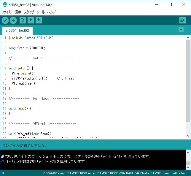
#include "si5351a3.h"

long freq = 7000000L;
//----------  Setup  ---------------
        
void setup() {
  Wire.begin();
  si5351aXtalCp(_8pF);     // 8pF set
  Vfo_out(freq);
}

//----------  Main Loop  ---------------

void loop() {
}

//----------  VFO out  ---------------        

void Vfo_out(long freq){
    si5351aSetFrequency(freq,_8mA);  // Strength 8mA set
}

si5351a3.hの内容


////////////////////////////////////////////////////////////////////////

// Author: Hans Summers, 2015
// Website: http://www.hanssummers.com
//
// A very very simple Si5351a demonstration
// using the Si5351a module kit http://www.hanssummers.com/synth
// Please also refer to SiLabs AN619 which describes all the registers to use
//----------------------------------------------------------------------
// Modifications: JA2GQP,2017/5/20
//     1)Output is CLK0 and CLK2.
//     2)Arduino and stm32duino Operable.
//     3)Storingth lebel. 2018/2/25
//     4)Xtal CP. 2018/2/25   
////////////////////////////////////////////////////////////////////////

#include <Wire.h>

#define CLK0_CTRL   16               // Register definitions
#define CLK1_CTRL   17
#define CLK2_CTRL   18
#define MSNA_ADDR   26
#define MSNB_ADDR   34
#define MS0_ADDR    42
#define MS1_ADDR    50
#define MS2_ADDR    58
#define PLL_RESET   177
#define XTAL_LOAD_C 183

#define R_DIV_1      0b00000000     // R-division ratio definitions
#define R_DIV_2      0b00010000
#define R_DIV_4      0b00100000
#define R_DIV_8      0b00110000
#define R_DIV_16     0b01000000
#define R_DIV_32     0b01010000
#define R_DIV_64     0b01100000
#define R_DIV_128    0b01110000

#define XTAL_CL    0b00010010
#define _0pF         0b00000000     // 0pF
#define _6pF         0b01000000     // 6pF
#define _8pF         0b10000000     // 8pF
#define _10pF        0b11000000     // 10pF

#define Si5351A_ADDR 0x60

#define _2mA         0b00000000     // 2mA
#define _4mA         0b00000001     // 4mA
#define _6mA         0b00000010     // 6mA
#define _8mA         0b00000011     // 8mA
#define CLK_SRC_PLL_A 0b00000000
#define CLK_SRC_PLL_B 0b00100000

#define XTAL_FREQ     25000400    // Crystal frequency for Hans' board

////////////////////////////////////////////////////////////////////////
// I2C write
////////////////////////////////////////////////////////////////////////

void Si5351_write(byte Reg , byte Data){
  Wire.beginTransmission(Si5351A_ADDR);
  Wire.write(Reg);
  Wire.write(Data);
  Wire.endTransmission();
}

////////////////////////////////////////////////////////////////////////
// Set up specified PLL with mult, num and denom
// mult is 15..90
// num is 0..1,048,575 (0xFFFFF)
// denom is 0..1,048,575 (0xFFFFF)
///////////////////////////////////////////////////////////////////////

void setupPLL(uint8_t pll, uint8_t mult, uint32_t num, uint32_t denom){
  uint32_t P1;                            // PLL config register P1
  uint32_t P2;                            // PLL config register P2
  uint32_t P3;                            // PLL config register P3

  P1 = (uint32_t)(128 * ((float)num / (float)denom));
  P1 = (uint32_t)(128 * (uint32_t)(mult) + P1 - 512);
  P2 = (uint32_t)(128 * ((float)num / (float)denom));
  P2 = (uint32_t)(128 * num - denom * P2);
  P3 = denom;

  Si5351_write(pll + 0, (P3 & 0x0000FF00) >> 8);
  Si5351_write(pll + 1, (P3 & 0x000000FF));
  Si5351_write(pll + 2, (P1 & 0x00030000) >> 16);
  Si5351_write(pll + 3, (P1 & 0x0000FF00) >> 8);
  Si5351_write(pll + 4, (P1 & 0x000000FF));
  Si5351_write(pll + 5, ((P3 & 0x000F0000) >> 12) | ((P2 & 0x000F0000) >> 16));
  Si5351_write(pll + 6, (P2 & 0x0000FF00) >> 8);
  Si5351_write(pll + 7, (P2 & 0x000000FF));
}

////////////////////////////////////////////////////////////////////////
// Set up MultiSynth with integer divider and R divider
// R divider is the bit value which is OR'ed onto the appropriate 
// register, it is a #define in si5351a.h
////////////////////////////////////////////////////////////////////////

void setupMultisynth(uint8_t synth, uint32_t divider, uint8_t rDiv){
  uint32_t P1;                          // Synth config register P1
  uint32_t P2;                          // Synth config register P2
  uint32_t P3;                          // Synth config register P3

  P1 = 128 * divider - 512;
  P2 = 0;                               // P2 = 0, P3 = 1 forces an integer value for the divider
  P3 = 1;

  Si5351_write(synth + 0, (P3 & 0x0000FF00) >> 8);
  Si5351_write(synth + 1, (P3 & 0x000000FF));
  Si5351_write(synth + 2, ((P1 & 0x00030000) >> 16) | rDiv);
  Si5351_write(synth + 3, (P1 & 0x0000FF00) >> 8);
  Si5351_write(synth + 4, (P1 & 0x000000FF));
  Si5351_write(synth + 5, ((P3 & 0x000F0000) >> 12) | ((P2 & 0x000F0000) >> 16));
  Si5351_write(synth + 6, (P2 & 0x0000FF00) >> 8);
  Si5351_write(synth + 7, (P2 & 0x000000FF));
}

////////////////////////////////////////////////////////////////////////
// Switches off Si5351a output
// Example: si5351aOutputOff(CLK0_CTRL);
// will switch off output CLK0
////////////////////////////////////////////////////////////////////////

void si5351aOutputOff(uint8_t clk){
  Si5351_write(clk, 0x80);              // Refer to SiLabs AN619 to see 
                                        //bit values - 0x80 turns off the output stage
}

////////////////////////////////////////////////////////////////////////
// Xtal cp
// Example: si5351aXtalCp(_8pF);
////////////////////////////////////////////////////////////////////////

void si5351aXtalCp(uint8_t cp){
  Si5351_write(XTAL_LOAD_C, XTAL_CL | cp); 
}

////////////////////////////////////////////////////////////////////////
// Set CLK0 output ON and to the specified frequency
// Frequency is in the range 1MHz to 150MHz
// Example: si5351aSetFrequency(10000000,_8mA);
// will set output CLK0 to 10MHz
//
// This example sets up PLL A
// and MultiSynth 0
// and produces the output on CLK0
////////////////////////////////////////////////////////////////////////

void si5351aSetFrequency(uint32_t frequency,uint8_t mA){
  uint32_t pllFreq;
  uint32_t xtalFreq = XTAL_FREQ;
  uint32_t l;
  float f;
  uint8_t mult;
  uint32_t num;
  uint32_t denom;
  uint32_t divider;

  divider = 900000000 / frequency;        // Calculate the division ratio. 900,000,000 is the maximum internal
                                          // PLL frequency: 900MHz
  if (divider % 2) divider--;             // Ensure an even integer 
                                          //division ratio

  pllFreq = divider * frequency;          // Calculate the pllFrequency: 
                                          //the divider * desired output frequency

  mult = pllFreq / xtalFreq;              // Determine the multiplier to 
                                          //get to the required pllFrequency
  l = pllFreq % xtalFreq;                 // It has three parts:
  f = l;                                  // mult is an integer that must be in the range 15..90
  f *= 1048575;                           // num and denom are the fractional parts, the numerator and denominator
  f /= xtalFreq;                          // each is 20 bits (range 0..1048575)
  num = f;                                // the actual multiplier is mult + num / denom
  denom = 1048575;                        // For simplicity we set the denominator to the maximum 1048575

                                          // Set up PLL A with the calculated  multiplication ratio
  setupPLL(MSNA_ADDR, mult, num, denom);
                                          // Set up MultiSynth divider 0, with the calculated divider.
                                          // The final R division stage can divide by a power of two, from 1..128.
                                          // reprented by constants SI_R_DIV1 to SI_R_DIV128 (see si5351a.h header file)
                                          // If you want to output frequencies below 1MHz, you have to use the
                                          // final R division stage
  setupMultisynth(MS0_ADDR, divider, R_DIV_1);
                                          // Reset the PLL. This causes a glitch in the output. For small changes to
                                          // the parameters, you don't need to reset the PLL, and there is no glitch
//  Si5351_write(PLL_RESET, 0x20);
                                          // Finally switch on the CLK0 output (0x4F)
                                          // and set the MultiSynth0 input to be PLL A 
  Si5351_write(CLK0_CTRL, 0x4C | mA | CLK_SRC_PLL_A);    // Strength lebel set
//  Si5351_write(CLK0_CTRL, 0x4C | CLK_SRC_PLL_A);    // Strength 2mA
}

////////////////////////////////////////////////////////////////////////
// Set CLK2 output ON and to the specified frequency
// Frequency is in the range 1MHz to 150MHz
// Example: si5351aSetFrequency2(10000000,_8mA);
// will set output CLK0 to 10MHz
//
// This example sets up PLL B
// and MultiSynth 1
// and produces the output on CLK2
////////////////////////////////////////////////////////////////////////

void si5351aSetFrequency2(uint32_t frequency,uint8_t mA){
  uint32_t pllFreq;
  uint32_t xtalFreq = XTAL_FREQ;
  uint32_t l;
  float f;
  uint8_t mult;
  uint32_t num;
  uint32_t denom;
  uint32_t divider;

  divider = 900000000 / frequency;        // Calculate the division ratio. 900,000,000 is the maximum internal
                                          // PLL frequency: 900MHz
  if (divider % 2) divider--;             // Ensure an even integer 
                                          //division ratio

  pllFreq = divider * frequency;          // Calculate the pllFrequency: 
                                          //the divider * desired output frequency

  mult = pllFreq / xtalFreq;              // Determine the multiplier to 
                                          //get to the required pllFrequency
  l = pllFreq % xtalFreq;                 // It has three parts:
  f = l;                                  // mult is an integer that must be in the range 15..90
  f *= 1048575;                           // num and denom are the fractional parts, the numerator and denominator
  f /= xtalFreq;                          // each is 20 bits (range 0..1048575)
  num = f;                                // the actual multiplier is mult + num / denom
  denom = 1048575;                        // For simplicity we set the denominator to the maximum 1048575

                                          // Set up PLL B with the calculated  multiplication ratio
  setupPLL(MSNB_ADDR, mult, num, denom);  
                                          // Set up MultiSynth divider 0, with the calculated divider.
                                          // The final R division stage can divide by a power of two, from 1..128.
                                          // reprented by constants SI_R_DIV1 to SI_R_DIV128 (see si5351a.h header file)
                                          // If you want to output frequencies below 1MHz, you have to use the
                                          // final R division stage
  setupMultisynth(MS2_ADDR, divider, R_DIV_1);
                                          // Reset the PLL. This causes a glitch in the output. For small changes to
                                          // the parameters, you don't need to reset the PLL, and there is no glitch
//  Si5351_write(PLL_RESET, 0x80);
                                          // Finally switch on the CLK1 output
                                          // and set the MultiSynth0 input to be PLL B 
  Si5351_write(CLK2_CTRL, 0x6C | mA | CLK_SRC_PLL_B);    // Strength lebel set
//  Si5351_write(CLK2_CTRL, 0x6C | CLK_SRC_PLL_B);    // Strength 2mA
}